India’s $11 Billion Semiconductor Push: Tata and ASML Partner for Dholera Fab
India is making a significant move into advanced semiconductor manufacturing with an $11 billion investment, partnering Tata Electronics with Dutch lithography giant ASML and Taiwan's PSMC to establish its first commercial 300mm wafer fabrication plant in Dholera, Gujarat.

India is embarking on a substantial initiative to bolster its domestic semiconductor manufacturing capabilities with an $11 billion investment. This strategic move involves a partnership between India’s Tata Electronics, the Netherlands-based ASML, a global leader in lithography equipment, and Taiwan’s Powerchip Semiconductor Manufacturing Corporation (PSMC). The collaboration aims to establish India’s first commercial 300mm wafer fabrication plant in Dholera, Gujarat, marking a pivotal step in the nation’s technological advancement beyond its traditional strengths in software and IT services.
The memorandum of understanding (MoU) for this venture was reportedly signed on May 16 during Indian Prime Minister Narendra Modi’s visit to the Netherlands, attended by Dutch Prime Minister Rob Jetten. This project is positioned to produce semiconductors for a wide array of sectors, including automotive, mobile devices, consumer electronics, connectivity, IoT, embedded memory, and other industrial applications. While India has been a key player in the global technology landscape, its direct involvement in advanced chip fabrication has been limited. This initiative signals a concerted effort to deepen its presence in the more complex and capital-intensive aspects of the technology supply chain.
Key facts:
- Investment: $11 billion
- Location: Dholera, Gujarat, India
- Partners: Tata Electronics, ASML, PSMC
- Wafer Size: 300mm
- Process Nodes: 28nm, 40nm, 55nm, 90nm, 110nm
- Target Applications: Automotive, IoT, consumer electronics, mobile, industrial
Technological Scope and ASML’s Role
The Dholera plant is designed to utilize 300mm silicon wafers, a standard industrial size for high-volume production. This dimension refers to the diameter of the silicon disc upon which multiple chips are fabricated, rather than the size of individual transistors. The partnership with PSMC is crucial, providing access to a technology portfolio that includes process nodes such as 28nm, 40nm, 55nm, 90nm, and 110nm. These nodes are critical for manufacturing a broad range of analog and logic chips essential for everyday electronics and industrial systems, rather than the bleeding-edge processors found in the most advanced AI accelerators or high-end consumer CPUs.
ASML’s involvement extends beyond merely supplying equipment. The Dutch company is expected to provide lithography tools and solutions, which are fundamental to transferring circuit patterns onto silicon wafers. This phase, known as lithography, is one of the most critical and complex steps in semiconductor manufacturing. ASML will also support the project through local talent training, supply chain resilience initiatives, and R&D infrastructure development. This comprehensive support aims to facilitate Tata’s industrial learning curve and enable the plant to scale its operations effectively.
It is important to note that while ASML is renowned for its state-of-the-art Extreme Ultraviolet (EUV) and High-NA EUV lithography systems, the current scope of the Dholera plant’s process nodes suggests the use of Deep Ultraviolet (DUV) lithography solutions. DUV technology is well-suited for the mature process nodes targeted by this project, which are vital for a vast market segment, even if they are not at the absolute forefront of transistor density. This aligns with ASML’s broader capabilities, demonstrating its role in supporting diverse stages of industrial maturity within the semiconductor sector.
Strategic Implications for India and Global Supply Chains
This investment is part of a larger Indian government strategy, which includes billions of dollars in subsidies to attract semiconductor and related manufacturing plants. The country currently has eight such projects underway, reflecting a national push to reduce reliance on foreign chip suppliers and to establish a more self-sufficient technological ecosystem. Prime Minister Modi has actively encouraged Dutch companies to invest in key sectors, including semiconductors, renewable energy, digital technologies, and healthcare, fostering closer economic ties.
From the Dutch perspective, companies like ASML are actively seeking new markets and geographical diversification. This strategy is increasingly critical in a global landscape marked by export controls and trade restrictions, particularly those stemming from technological rivalry between the United States and China. Expanding into new regions helps de-risk supply chains and opens up new avenues for growth and collaboration.
For ReviewArticle readers, this development signifies a shift in the global technology landscape. While India may not immediately compete at the cutting edge of semiconductor technology with nations like Taiwan or South Korea, this move establishes a foundational capability for large-scale chip production. The focus on proven processes and sustained demand for chips in automotive, IoT, and consumer electronics means a more robust and diversified supply chain for these critical components. This initiative can enhance the resilience of global tech manufacturing and offer new opportunities for product developers and businesses relying on these widely used semiconductor components. It also underscores the importance of mature node technologies, which are often overlooked in the race for the smallest transistors but form the backbone of countless everyday devices and industrial systems.
Source: Xataka IA – https://www.xataka.com/empresas-y-economia/11-000-millones-dolares-gigante-europeo-asi-prepara-india-su-proximo-gran-salto-industria-chips
Source
Xataka IA Publicacion original: 2026-05-21T06:31:39+00:00
Related articles
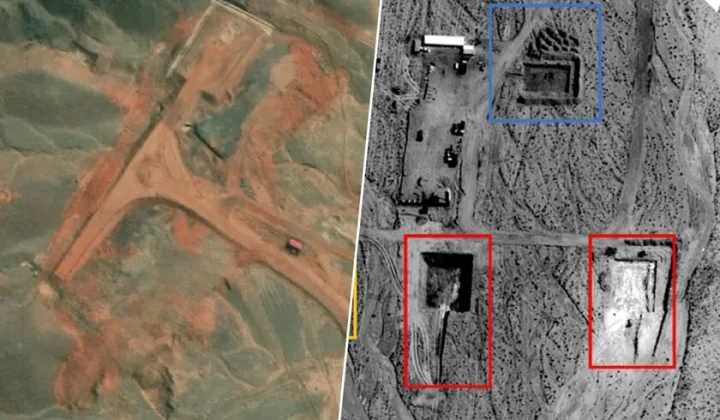
Satellite Images Reveal Mysterious Chinese Desert Structures Aimed at Taiwan
New satellite imagery from China's Jilantai base shows two unidentified rectangular structures with retractable roofs, sparking speculation about their purpose and potential…
Read article
Claude 3.5 Sonnet: A Leap in AI Model Performance and Accessibility
Anthropic's latest AI model, Claude 3.5 Sonnet, promises significant improvements in speed, cost-effectiveness, and capability, marking a new milestone in accessible AI.
Read article
Cold Water Digestion Myth Debunked by Experts: It Slows, Not Stops
While drinking ice-cold water doesn't block digestion, experts explain it can lead to slower, less comfortable digestive processes.
Read article
Claude 3.5 Sonnet: A Leap in AI Performance for Developers and Businesses
Anthropic's latest model, Claude 3.5 Sonnet, offers significant improvements in speed and cost-effectiveness, making advanced AI capabilities more accessible to developers and…
Read articleWiki relacionada
Understanding Large Language Models (LLMs)
An introduction to Large Language Models (LLMs), their architecture, capabilities, limitations, and real-world applications in AI.
Read article
Understanding LLM Context Windows
An in-depth look at Large Language Model context windows, their importance, limitations, and how they impact AI applications.
Read article
Comprendiendo los Modelos Llama 3: Una Visión Integral
Explore la familia de modelos Llama 3, detallando su arquitectura, capacidades, limitaciones y aplicaciones prácticas en el desarrollo de IA.
Read article
Comprensión de los Modelos de Lenguaje Grandes (LLM)
Una mirada en profundidad a los Modelos de Lenguaje Grandes (LLM), su arquitectura, capacidades, limitaciones e impacto en el desarrollo de la…
Read article