
IBM Achieves Sub-Nanometer Chip Milestone, Ushering in New Era for AI and Computing
IBM has successfully developed the world's first chip utilizing sub-nanometer technology, a 0.7nm node, promising significant boosts in performance and energy efficiency crucial for advanced AI and cloud infrastructure.
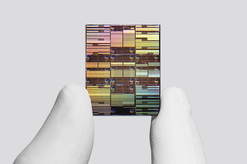
IBM has announced a significant leap in semiconductor technology, unveiling what it claims is the world’s first chip manufactured using sub-nanometer processes. This groundbreaking chip operates on a 0.7-nanometer (7-angstrom) node, a scale that enables the integration of nearly 100 billion transistors within a space no larger than a fingernail. This achievement represents a critical step beyond the long-standing scaling challenges faced by the industry as transistors approach atomic dimensions.
The development addresses the evolving landscape of semiconductor manufacturing, which has long been guided by Moore’s Law. This observation predicted the exponential growth in transistor density on integrated circuits. However, as transistors near the size of individual atoms, quantum effects introduce significant hurdles to further miniaturization. IBM’s innovation suggests a new pathway forward, moving beyond incremental shrinking of existing designs to a fundamental reimagining of chip architecture and construction.
Enhanced Performance and Efficiency
The new 0.7nm chip from IBM demonstrates substantial improvements in computational capabilities. It offers up to a 50% increase in performance when compared to IBM’s own 2nm circuits. Alternatively, it can deliver up to 70% greater energy efficiency. This dual benefit provides designers with significant flexibility to tailor the chip’s characteristics for specific applications. For demanding tasks such as generative artificial intelligence (AI), cloud infrastructure, and next-generation devices, this adaptability is vital for enabling truly transformative computing power.
Introducing the Nanostack Architecture
Central to this sub-nanometer chip’s design is IBM’s proprietary nanostack technology. This architecture is characterized as the industry’s first three-dimensional design based on stacked nanosheets. It builds upon prior advancements in nanosheet technology, which themselves represented an evolution from FinFET transistors by employing multiple stacked horizontal silicon sheets wrapped by a control gate. This arrangement enhances electrical performance within a more compact form factor.
Nanostack takes this concept further by enabling the staggered stacking of entire transistors in three dimensions, leveraging 3D sequential integration to pack more logic onto a smaller surface area. A key differentiator of this architecture is its ability to incorporate different material combinations in each stacked layer. This granular approach allows for the optimization of individual transistor performance and energy efficiency independently.
The flexibility afforded by nanostack means that not all transistors on a chip need to operate with the same priorities. Some can be configured for maximum speed, while others can be optimized for power saving. This layer-by-layer tuning capability, which is not possible with the same precision in planar or conventional nanosheet architectures, allows for a more nuanced balance of performance and efficiency tailored to specific computational needs.
IBM also presented findings at the VLSI 2026 conference demonstrating a 40% improvement in SRAM scaling attributed to the nanostack architecture. This enhancement is crucial for developing semiconductors capable of handling the high bandwidth demands of the most intensive AI workloads.
Technical Validation
The experimental validation of the nanostack architecture rests on three core pillars: ultrafine dielectric bonding in CMOS integration, demonstration of dual-channel engineering capabilities, and the functional operation of a CMOS inverter exhibiting expected switching performance. The functional CMOS inverter is particularly significant, as it represents the most basic logic unit in any digital circuit. The successful execution of this fundamental component by nanostack with forecasted metrics confirms that the architecture is not merely a theoretical concept but a physically realizable technology ready for practical implementation in computing systems.
Manufacturing and Future Outlook
IBM, in collaboration with partners Lam Research, Tokyo Electron, and SCREEN Semiconductor Solutions, has been working extensively on the necessary tools and manufacturing processes, utilizing ASML’s High NA extreme ultraviolet lithography at its Albany, New York facilities.
However, the transition from laboratory breakthrough to mass production is a lengthy process. IBM anticipates that the first commercial adoption of nanostack technology at the sub-nanometer node will occur within three to five years. Further scaling of the technology is projected to take at least another decade.
IBM also recently announced Anderon, an independent quantum chip manufacturing company that aims to combine expertise in quantum computing and semiconductors for industrial-scale quantum wafer production.
With its 7-angstrom node achievement, IBM not only demonstrates the physical possibility of the sub-nanometer scaling era but also reinforces its position as a leading research laboratory in an industry continually seeking to overcome the physical limits of silicon.
Key Facts
| Detail | Information | Source |
|---|---|---|
| Chip Size | 7nm (7 angstroms) | Xataka IA |
| Transistor Count | Nearly 100 billion | Xataka IA |
| Key Technology | nanostack (3D stacked nanosheet architecture) | Xataka IA |
| Performance Gain | Up to 50% vs. 2nm chips | Xataka IA |
| Energy Efficiency Gain | Up to 70% vs. 2nm chips | Xataka IA |
| Commercialization Timeline | 3-5 years for initial adoption | Xataka IA |
What Remains Unclear
While IBM has demonstrated a functional prototype and outlined its technical validation, the specific materials used in the stacked layers beyond silicon, and the precise challenges and solutions encountered during the development of the dual-channel engineering and ultrafine dielectric bonding remain areas for further detail. The exact roadmap for the decade of additional scaling beyond initial commercialization is also not fully specified.
Source: https://www.xataka.com/investigacion/primer-chip-1-nm-esta-aqui-ha-fabricado-ibm-espectacular
Source
Xataka IA Publicacion original: 2026-06-25T10:01:32+00:00
Related articles

IBM CEO Puts a Number on the Open-Weight AI Value Proposition: 90% of the Performance at 10% of the Token Cost
IBM CEO Arvind Krishna told analysts that open-weight models now deliver about 90% of frontier-model effectiveness while costing between 10% and 25%…
Read article
OCU Finds Spanish Homeowner Communities Overpaying Up to €1,500 on Electricity and €3,515 on Gas—Can AI Tools Optimize Shared Energy Bills?
A new OCU analysis of Spanish homeowner community bills reveals widespread overpayment due to non-competitive tariffs and excess contracted power. Could AI-driven…
Read article
Mayotte fiber dispute does not meet ReviewArticle’s AI news brief
Le Monde reports that France’s competition authority has ordered Orange to suspend part of its fiber-optic rollout in Mayotte. The dispute is…
Read article
DiffEEG Model Uses Diffusion Pre-Training to Improve Seizure Detection from Minimal Labeled Data
Researchers have introduced DiffEEG, a 9.6-million-parameter foundation model that combines denoising diffusion pre-training with reinforcement learning fine-tuning to detect seizure events from…
Read articleWiki relacionada

AI Model API Pricing and Context Window Comparison: Current Rates and Limits
Compare the latest API pricing, context windows, and capabilities of leading AI model providers including OpenAI, Anthropic, Google, and Mistral. Practical guidance…
Read article
AI Agent Evaluation Frameworks: How to Benchmark Agentic Systems
A practical guide to evaluating AI agents — from task completion metrics to safety, cost, and robustness. Covers major frameworks, primary sources,…
Read article
LLM Benchmarks Decoded: What MMLU, HumanEval, and GSM8K Actually Measure for Developers
A developer-focused breakdown of the most-cited LLM benchmarks — MMLU, HumanEval, GSM8K, MATH, Chatbot Arena — including what they test, their hidden…
Read article
What Is RAG? A Practical Guide to Retrieval-Augmented Generation in 2025
Retrieval-Augmented Generation (RAG) grounds LLM outputs in external data, reducing hallucinations and enabling enterprise use cases. This guide covers how RAG works,…
Read article